Analysis of Magnetic and Thermal Semiconductor Power Modules
| Topics covered in this article: |
| Ⅰ. Magnetic and Thermal analysis of Power Modules |
| Ⅱ. Extraction of the Proposed Model |
| Ⅲ. Simulations and Results |
| Ⅳ. Conclusion |
Over the past few years, semiconductor technology has come a long way, especially in the fields of power electronics with applications in research and heavy industry applications. Insulated-gate bipolar transistor (IGBT) modules play a crucial role as they are implemented in applications with high operating temperatures, fast switching speeds, higher reliability, etc. In such situations, getting precise results is of utmost importance as there may be several dangerous outcomes to the circuits or even the users operating the circuits if not calculated correctly.
Ⅰ. Magnetic and Thermal analysis of Power Modules
The experiment conducted presents a simulation wherein, the electrical, thermal and magnetic characteristics of the IGBT are tested during the circuit operations.

Fig 1: Schematics of the proposed EM-electro-thermal analysis method.
The parasitic properties between the chip surfaces (collectors, emitters, and gates) and the module external terminals are represented by this electromagnetic network. The electro-thermal IGBT chip model is constructed in the circuit representing the working point conditions dependency using curve-fitting and weighted interpolation of experimental test results or data sheets. This electro-thermal model acts as an important link between the thermal and EM networks, having to accept Tj s information from each chip and returning power loss values to the former, and accepting existing information and restoring chip on-state voltage drop (Vce(on)) values to the latter.

Fig 2: 1700V/450A half-bridge IGBT power module layout.
The data on the frequency dependant resistance and inductance values between external terminals and chip surfaces, such as from the module's DC+ power terminal to the collector surfaces of the high-side switch IGBT chips is included as shown in Fig 2.
Ⅱ. Extraction of the Proposed Model
Until recent times, research on the self-consistent interaction between the electrical and thermal characteristics of power modules has been an exciting topic as it includes technologies which can be used in overcoming several obstacles using the ROM method.
While conducting the tests, all thermal characteristics were considered along with an assumption of an intact cooling boundary at the bottom for further simplification and efficiency. Moreover, a baseplate temperature of 90![]() was set during the simulation of the bottom process.
was set during the simulation of the bottom process.


Fig 3: Temperature distribution when power loss is applied only to U5
As shown above, Fig 3 depicts the thermal behaviour of the entire packaging structure which was recorded to study accurate electro-thermal coupling.

Fig 4: Comparing results of Icepack SVM, Simplorer thermal network and experimentation test
Fig 4 shows the effectiveness of the extraction process to demonstrate its comparison with different results. For instance, the comparison was done among Icepak FVM simulation, Simplorer thermal network simulation and experimental test results to check the thermal resistance of the low side switch. The graph with thermal network topologies shows identical simulation results as that of the standard FVM simulation. The current sharing properties of the IGBT depend on the frequency of the parasitic components of the module packaging which also includes the resistance and inductance of the conduction paths. During its application, each conduction path from the external bus bar terminals to the chip surfaces in the IGBT module application may have an effect on how current is spread among the chips and how each chip switches by itself. This makes it very important for the modules to characterize the parasitic values from all external terminals to the surfaces of each chip.
Ⅲ. Simulations and Results
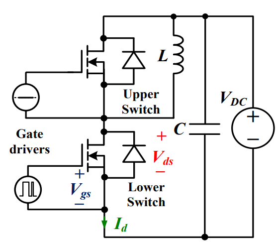
Once the extraction process of the IGBT chip model is complete, simulations for the thermal and EM networks and their analytical representations are taken into consideration for the study of their module performance in chopper circuits. In such chopper circuits, while IGBT modules are operating at high frequencies, a 900V DC power supply is set with a load connected in parallel to the high side switch for three IGBT switches and three FRD chips
Analytical Solution: In a chopper circuit, it is very important to take into account the current sharing and temperature dependency of the power losses due to which the loss can be viewed in an analytic solution.
𝑃𝑠𝑤,𝐼𝐺𝐵𝑇 = (𝐸𝑜𝑛 + 𝐸𝑜𝑓𝑓) ⋅ 𝑓𝑠w
From the above equation, 𝐸𝑜𝑛 and 𝐸𝑜𝑓𝑓 is the turn on and turn off of the IGBT chip at a set 90℃ and 𝑓𝑠w is the switching frequency.
Electro-Thermal Simulation: As shown in the below figure, an addition of a thermal network above the electrical simulation was used in getting the simulated output. The temperature-sensitive electrical properties of the chips, such as the loss energy and Vce(on) values, can be dynamically updated by linking the thermal pins of the electro-thermal chip model to the thermal network. This enables the power losses calculated from the circuit simulation to be supplied into the thermal network.

Fig 5: Electro thermal simulation topology
EM-Electro-Thermal Simulation
As seen above, the thermal and EM networks which show the different imbalances in impedance and parasitic components should always be reviewed for smooth operations. Networks with zero-dimensional setups were also utilized in the EM-electro-thermal analysis.

Fig 6: EM-electro-thermal simulation topology.
In Fig 6, the EM and thermal networks are integrated together in the simulation circuit. Using EM networks, the IGBT chip electro-thermal models are embedded into the application circuit during the working.

Fig 7: Simulation results (a) Gate driver voltage and Vge of chips (b) IGBT chip current values (c) IGBT chip averaged total power losses (d) IGBT chip Tj variation.
In figure 7, the simulated outputs in different conditions and temperatures are shown for further understanding of the IGBT and its performance. The IGBT chip U6 in Fig. 11 (a) has the highest Vge value due to its proximity to the module packaging's gate control terminals, Figure 7 (b) displays the current distribution among the three paralleling chips. As per Fig. 11, Chip U6 describes the highest averaged total power loss (c) and In Fig. 7, the Tj variation over time is depicted (d). If there are temperature instabilities in the IGBT, there are various possibilities for long-term issues which may increase power loss and thermal stress.
Ⅳ. Conclusion
The behaviour of IGBT semiconductor power modules with the EM-Electro-Thermal coupling, along with current sharing properties and thermal characteristics was studied. The simulation results conducted were achieved perfectly as per the prediction making it further scalable in various physical and electronic domains. With the results obtained, it can be said that there are higher chances to reveal the effects of IGBT power module packaging on the electro-thermal behaviour of the chips. With more extensive research on this topic, such systems can even be deployed in complex devices and have enhanced reliability.

 Discovering New and Advanced Methodology for Determining the Dynamic Characterization of Wide Bandgap DevicesSaumitra Jagdale15 March 20242498
For a long era, silicon has stood out as the primary material for fabricating electronic devices due to its affordability, moderate efficiency, and performance capabilities. Despite its widespread use, silicon faces several limitations that render it unsuitable for applications involving high power and elevated temperatures. As technological advancements continue and the industry demands enhanced efficiency from devices, these limitations become increasingly vivid. In the quest for electronic devices that are more potent, efficient, and compact, wide bandgap materials are emerging as a dominant player. Their superiority over silicon in crucial aspects such as efficiency, higher junction temperatures, power density, thinner drift regions, and faster switching speeds positions them as the preferred materials for the future of power electronics.
Read More A Comprehensive Guide to FPGA Development BoardsUTMEL11 September 202515620
This comprehensive guide will take you on a journey through the fascinating world of FPGA development boards. We’ll explore what they are, how they differ from microcontrollers, and most importantly, how to choose the perfect board for your needs. Whether you’re a seasoned engineer or a curious hobbyist, prepare to unlock new possibilities in hardware design and accelerate your projects. We’ll cover everything from budget-friendly options to specialized boards for image processing, delve into popular learning paths, and even provide insights into essential software like Vivado. By the end of this article, you’ll have a clear roadmap to navigate the FPGA landscape and make informed decisions for your next groundbreaking endeavor.
Read More Applications of FPGAs in Artificial Intelligence: A Comprehensive GuideUTMEL29 August 20253823
This comprehensive guide explores FPGAs as powerful AI accelerators that offer distinct advantages over traditional GPUs and CPUs. FPGAs provide reconfigurable hardware that can be customized for specific AI workloads, delivering superior energy efficiency, ultra-low latency, and deterministic performance—particularly valuable for edge AI applications. While GPUs excel at parallel processing for training, FPGAs shine in inference tasks through their adaptability and power optimization. The document covers practical implementation challenges, including development complexity and resource constraints, while highlighting solutions like High-Level Synthesis tools and vendor-specific AI development suites from Intel and AMD/Xilinx. Real-world applications span telecommunications, healthcare, autonomous vehicles, and financial services, demonstrating FPGAs' versatility in mission-critical systems requiring real-time processing and minimal power consumption.
Read More 800G Optical Transceivers: The Guide for AI Data CentersUTMEL24 December 20254516
The complete guide to 800G Optical Transceiver standards (QSFP-DD vs. OSFP). Overcome supply shortages and scale your AI data center with Utmel Electronic.
Read More Xilinx FPGAs: From Getting Started to Advanced Application DevelopmentUTMEL09 September 20254418
This guide is your comprehensive roadmap to understanding and mastering the world of Xilinx FPGA technology. From selecting your first board to deploying advanced AI applications, we'll cover everything you need to know to unlock the potential of these remarkable devices. The global FPGA market is on a significant growth trajectory, expected to expand from USD 8.37 billion in 2025 to USD 17.53 billion by 2035. This surge is fueled by the relentless demand for high-performance, adaptable computing in everything from 5G networks and data centers to autonomous vehicles and the Internet of Things (IoT). This guide will walk you through the key concepts, tools, and products in the Xilinx ecosystem, ensuring you're well-equipped to be a part of this technological revolution.
Read More
Subscribe to Utmel !
![FM31L276-G]() FM31L276-G
FM31L276-GCypress Semiconductor Corp
![MCS3122T-I/ST]() MCS3122T-I/ST
MCS3122T-I/STMicrochip Technology
![SI8230BB-D-IS]() SI8230BB-D-IS
SI8230BB-D-ISSilicon Labs
![HCS365-I/SM]() HCS365-I/SM
HCS365-I/SMMicrochip Technology
![CAP014DG]() CAP014DG
CAP014DGPower Integrations
![FM31278-GTR]() FM31278-GTR
FM31278-GTRCypress Semiconductor Corp
![ACNW3130-000E]() ACNW3130-000E
ACNW3130-000EBroadcom Limited
![ACPL-3130-300E]() ACPL-3130-300E
ACPL-3130-300EBroadcom Limited
![HCS410/P]() HCS410/P
HCS410/PMicrochip Technology
![L9654TR]() L9654TR
L9654TRSTMicroelectronics


 Product
 Brand
Brand Articles
 Tools
Tools


